Conventional gold bump bonding requires one of the bonding chips to be prepared with gold studs. Double gold stud bump bonding requires both chips to be studded with gold, coined, and then bonded. While this adds extra steps to the bonding process, this technique remedies several draw-backs for conventional single gold stud bump bonding. The typical pressure and temperature required for thermo-compression can be hazardous to sensitive circuitry. Also, devices that require a very high numbers of gold-studs will consequently require a very high pressure to bond, which can exceed the capability of the aligner bonder. Similarly, the high temperature required can weaken bonds of other interconnects, such as solder bumps, if they were in place before the gold bond.
Stud-to-stud thermo-compression completes the bond. If the contact during the bonding were to be made between two semi spherical gold-studs, there would likely be slippage or inadequate contact due to minor misalignment. To work around this, the studs on one or both devices can be coined. This creates a better surface for contact, which greatly improves bond yield. Once this step is completed, the devices to be bonded are aligned and bonded through thermo-compression.
First, gold-studs are formed using a Westbond ball bonder, which is equipped with a ceramic capillary. Then, the gold-stud can be flattened through a process called “coining”, a technique that involves compressing the studs over a flat piece of silicon with roughly 140 g/stud, at room temperature. On the left is a gold stud that is uncoined, and on the right is a stud that has been coined. Notice that all semblance of the uncoined stud's distinguishing features have morphed to create a flat, wide plateau.
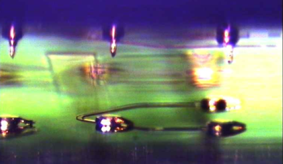
The chips are bonded through a thermo-compression cycle on the Finetech pico ma. In order to test the viability of double studding as an interconnect technique, the parameter space of temperatures and pressures for bonding was explored. To test the resistance of the double stud bonds, dummy chips with an array of 20 pads, each with traces allowing a four-point (Kelvin) measurement of the bond resistance were used. Because gold studs are formed with a manual gold ball bonder, twenty pads provide sufficient statistics for our investigations without demanding a superfluous amount of time on the machine. Both chips had gold-studs placed on the bond pads, and both sides were coined at 140 g/stud. Once the samples were properly prepared, we bonded pairs of chips under varying conditions using the Finetech flip-chip bonder. The image below shows a side view moments before the bond is created. The top chip (dark purple region on the top of the photo) with three gold studs poking down is hovering just above the bottom chip (green middle to the bottom of the picture. Visible on the bottom chip are the mating gold studs (4 visible total, with 3 of them connected by a U-shaped trace).
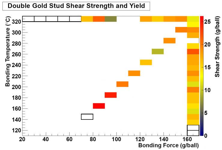
Once the bonds were completed, those with 100% yield were tested for shear strength using a force meter pulling the chips apart until the bond was broken. We define 100% yield as an assembly in which none of the bonds has a resistance > 0.5 Ω. This image shows a graphical representation of the results from the Bonding Parameter Exploration tests of double gold studs. The plot shows the amount of force and heat used during each bond, with the colored squares corresponding to bonds with a yield of 100%, and the clear squares with black outlines being bonds with less than 100% yield. The color of the squares corresponds to the amount of force required to shear the bond formed under those parameters. The blank spots at 100-110 g/stud at 320 °C are bonds that fell apart before the shear test.
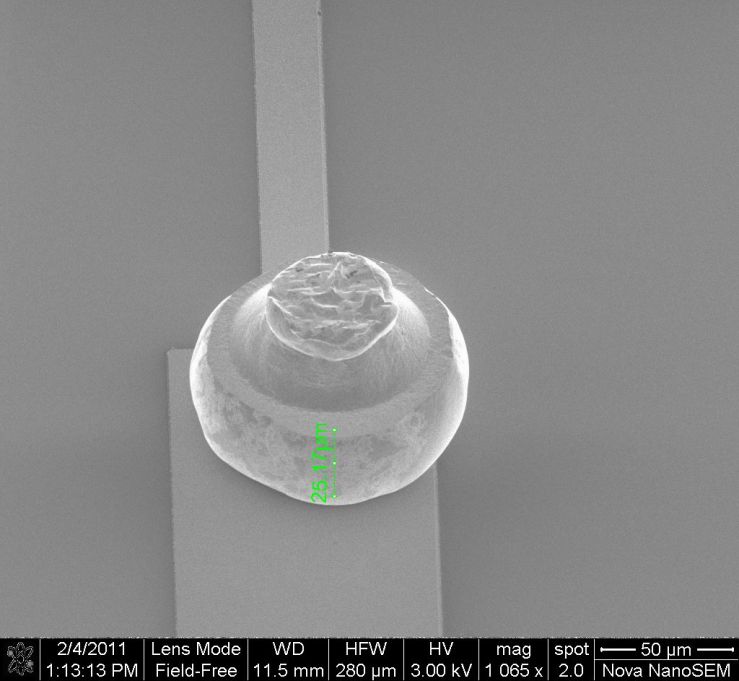
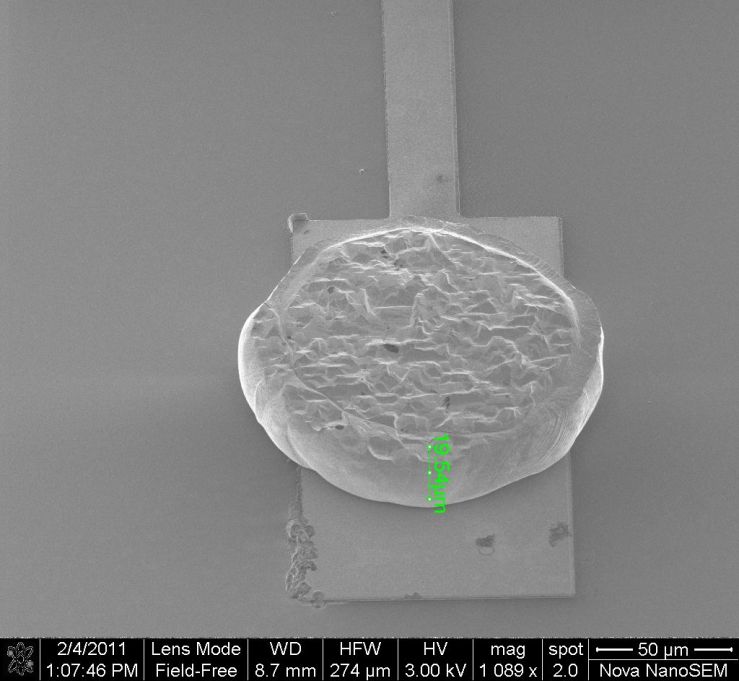
The pulling tests revealed that most bonds had shear strengths of roughly 15 g/stud, though the bonds with a combination of low temperature and pressure had shear strengths closer to 25 g/stud. This unexpected behavior may be explained by another factor. In most cases the values are lowerlimits on the stud-to-stud interface’s actual shear strength, as most breaks occurred at the stud to chip connection rather than the stud-to-stud contact. This is illustrated in Figure 5. In many cases during the shear test the studs pulled off parts of the underlying pads and even chunks of silicon from the chip, indicating that double stud connections are quite strong. Hence, we conjecture that as the temperature of the bonding process increased, the strength of the pad to oxide substrate connection was somehow weakened.